產品介紹
-
-
NANOEDUCATOR II
AFM holds a strong positions in scientific research as is used as a routine analytical tool for physical properties characterization with high spatial resolution down to atomic level. Solver Nano is the best choice for scientists who are need a single instrument that is an affordable, robust, user-friendly and professional tool.
產品說明
產品應用
Why is nanotechnology interesting for education?
Cutting edge achievements in science and most successful R&D projects in commercialization are on an interdisciplinary level, combining physics – chemistry –biology - mathematics – engineering – technology - IT. The earliest, widespread description of nanotechnology refers to the particular technological goal of precisely manipulating atoms and molecules for fabrication of macroscale products. Proceeding further down to atomic scale, where no border between the scientific disciplines exist and all of them are essential for developers and scientists to understand the technological processes.
Thus using this interdisciplinary approach to the education of students provides a very effective integration and coaches graduate students to fit into an innovative national economy. Scientific projects (school science, pre- college science and etc.) allow to cope with interdisciplinary connections, develop an interdisciplinary approach, form systematically scientific thinking and learn more about modern problems of physics, chemistry, biology and nanotechnology. This is the one of the mission of STEM centers.
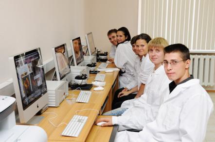
Laboratory work of students speciality “Nanomaterials”.
In the new scientific world of nanotechnology a widespread opinion persist that there are two important modern developments: the atomic force microscope (AFM) and the scanning tunnel microscopy (STM). Those are the instruments that have launched nanotechnology due to the fact that scanning probe microscopes are not limited by the wavelength of sound or light and can achieve high resolution results under a variety of environmental conditions..
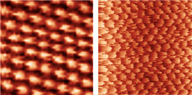
HOPG atomic resolution, STM scan size 2×2 nm. Solver Nano on 100x100 um CL scanner.
SOLVER Nano is enabled for teaching principles of scanning probe microscopy and acquiring skills for studying nanoobjects and microstructures. Students can also perform all modern AFM and STM techniques with SOLVER Nano:
In Air: AFM (contact and intermittent contact), AFM spectroscopy, AFM lithography (force, current, voltage), Lateral Force Microscopy, Force Modulation Microscopy, Spreading Resistance Imaging, Piezoresponce Force Microscopy and Switching Spectroscopy, EFM, Kelvin Probe Force Microscopy, MFM, STM (microscopy, spectroscopy, lithography).
In liquid: Contact and Amplitude Modulation AFM, AFM Spectroscopy, AFM Force Lithography, Lateral Force Microscopy.
SOLVER Nano for education provides complete didactic materials for different skill levels of young aspiring scientists.
Basic level: to demonstrate various phenomena and develop skills to work on modern equipment.
Advanced level: designed for advanced studies with higher skilled students to provide insights on composite nature of modern research and interdisciplinary connections.
Research level: performed individually. Example are given on actual problems to demonstrate the structure of scientific research, form skills of designing and performing experiments, work with scientific advisers – tutors and prepare to engage in independent research.
產品規格
| Atomic Force Microscopy Contact AFM Constant Height mode Constant Force mode Contact Error mode Lateral Force Imaging Spreading Resistance Imaging Force Modulation microscopy Piezoresponse Force Microscopy Amplitude modulation AFM Intermittent contact mode Phase Imaging mode Semicontact Error mode Non-Contact mode Electrostatic Force Modes Contact EFM EFM Scanning Capacitance Microscopy Kelvin Probe Force Microscopy MFM DC MFM AC MFM Dissipation Force Microscopy |
AFM Spectroscopies Force-distance curves Adhesion Force imaging Amplitude-distance curves Phase-distance curves Frequency-distance curves Full-resonance Spectroscopy STM techniques Constant Current mode Constant Height mode Barrier Height imaging Density of States imaging I(z) Spectroscopy I(V) Spectroscopy Lithographies AFM Oxidation Lithography STM Lithography AFM Lithography - Scratching AFM Lithography - Dynamic Plowing HD Modes |
General specs:
| Scanner | 100 x 100 x 12 um closed loop scanner, 3x3x3 um open loop scanner. |
| AFM resolution | 0.01 nm. |
| Environments | Air and liquid measurements. |
| Combined video optical microscopes | Build in 100x optical USB microscope. External 500x optical microscope. |
| Design | Table-top, affordable, robust and user-friendly |
Scanner |
|
| Scanning field | High voltage regime: 100x100x12 um. Low voltage regime: 3x3x3 um. |
| Scanner type | Metrological piezotube XYZ scanner with sensors. |
| Sensors type | XYZ – ultrafast capacitance sensors. |
| Sensors noise | Low noise XY sensor: < 0.3 nm. Metrological Z sensor: < 0.03 nm. |
| Sensors linearity | Metrological XY sensor: < 0.1% Metrological Z sensor: < 0.1 % |
| Overall scanner parameters | 100x100x12 um with CL. Resolution: XY -0.3 nm, Z – 0.03 nm. Linearity: XY - < 0.1%, Z - < 0.1%. 3x3x3 um with OL. Resolution: XY -0.05 nm, Z – 0.01 nm. |
Sample |
|
| Sample positioning range | 12 mm. |
| Sample positioning resolution | 1.5 um. |
| Sample dimension | up to 1,5” X 1,5” X 1/2”, 35x35x12 mm |
| Sample weight | up to 100 g. |
| Approach system type | Z – Stepper Motor |
| Approach system step size | 230 nm. |
| Approach system speed rate | 10 mm per min |
| Algorithm Gentle approach | Available (probe guaranteed to stop before it touches the sample) |
Scanning Heads |
|
| AFM head for Si cantilever | Available. All commercial cantilevers can be used |
| Type of cantilever detection | Laser/Detector Alignment |
| Probe holders | Probe holder for air measurements. Probe holder for liquid measurements. |
| Type of AFM head mounting | Cinematically mount. Mount accuracy 150 nm. (Remove/mount accuracy) |
| STM AFM head for wire probes | Available. Tungsten wire for AFM measurement. (low cost experiments) Pt|Ir wire for STM measurements. |
| Type of cantilever detection | Piezo for AFM measurement. |
| Probe holders | Probe holder for air and liquid measurements. |
Controllers. Digital professional controller |
|
| Number of images can be acquired during one scanning cycle | Up to 16 |
| Image size | Up to 8Kx8K scan size |
| ADC | 500 kHz 16-bit ADC 12 channels (5 channels with software controlling gain amplifiers 1,10,100,1000) Individual filter on each channel |
| DSP | Floating point 320MHz DSP |
| Digital FB | Yes 6 Channels |
| DACs: | 4 composite DACs (3x16bit) for X,Y,Z, Bias Voltage 2 16-bit DAC for user output |
| XYZ scanner control voltage | High-voltage outputs: X, -X, Y, -Y, Z, -Z at -150 V to +150 V Low-voltage mode XY ± 10 V |
| XY RMS noise in 1000 Hz bandwidth | 0.3 ppm RMS |
| Z RMS noise in 1000 Hz bandwidth | 0.3 ppm RMS |
| XY bandwidth | 4 kHz (LV regime – 10 kHz) |
| Z bandwidth | 9 kHz |
| Maximal current of XY amplifiers | 1.5 mA |
| Maximal current of Z amplifiers | 8 mA |
| Integrated demodulator for X,Y,Z capacitive capacitance sensors | Yes |
| Open/Closed-loop mode for X,Y controlх | Yes |
| Generator frequency setting range | DC – 5 MHz |
| Deflection registration channel bandwidth | 170 Hz-5 MHz |
| Lateral Force registration channel bandwidth | 170 Hz -5 MHz |
| 2 additional registration channel bandwidth | 170 Hz -5 MHz |
| Bias Voltage | ± 10 V bandwidth 0 – 5 MHz |
| Modulating signals supply | To the probe (external output); High-voltage X,Y, Z channels (including LV regime); Bias Voltage. |
| Number of generators for modulation, user accessible | 2, 0-5 MHz, 0.1 Hz resolution |
| Stepper motor control outputs | Two 16-bit DACs, 20 V peak-to-peak, max current 130 mA |
| Additional digital inputs/ outputs | 6 |
| Additional digital outputs | 1 |
| I2C bus | Yes |
| Macro language | |
| Max. cable length between the controller and SPM base or measuring heads | 2 m |
| Computer interface | USB 2.0 |
| Voltage supply | 110/220 V |
| Power consumption | ≤ 110 W |
Software for SPM operation and Data processing.
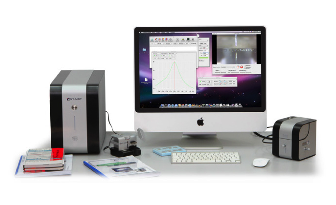
Software written by programmers NT-MDT and specialized management probe microscopes and associated devices (external and build-in) and also signal and image processing obtained with SPM. This software is used to manage all SPM from NT-MDT, but adapted for each model (Next, Ntegra, Solver Nano). In the case of use with Solver Nano, the software interface as much as possible easy and user-friendly.
Operation Interface
- User-defined configurable GUI
- Basic and advanced GUI layouts
- Handy hardware configuration wizard
- Quick access for all main parameters
- Quick access to customized scripts
- Automatic single-click setup for all available techniques
- Interactive Help system
Laser alignment
- Handy indication for laser alignment
Resonance
- Automatic configuration for standard probes
- Automatic resonance tune and phase adjustment
Approach
- Automatic routine for tip-sample engagement
- Soft Approach gentle engagement routine
- Handy stepper motor control
- Real time engagement oscilloscope
Scan
- Up to 8 sumultaneous signal channels
- Up to 8K points
- Automated single-click scanning mode setup
- Handy scan area selection tool
- Two pass techniques
- Cyclic mode
- Pause tool
- PreScan regime
- OverScan regime
- Angle scanning
- Non-square pixel mode
- Live 3D view
- Quick access to main scanning parameters via Parameters panel
- Quick access to main tuning operations via Quick panel
- Automatic PID setup
- Adaptive scan
- Cross-sections for each and all scans
- Full-screen mode
Curves
- Variety of standard modes
- Available arguments: Height, BV, Frequency, SetPoint
- Up to 3 channels measured simultaneously
- Limits for each channel
- Independent setup for resolution and speed for trace and retrace
- Point/Multi Point/Line/Grid measurement modes
Lithography
- Vector/Raster techniques
- Constant/Pulse/Gradient regimes
- Force/Voltage/Current modes
- Handy CAD for vector lithography
- Support for main graphical standards for raster lithography
- Scan Area / Litho Mask transparent overlay
Tools
- Oscilloscope
- Real time signal control
- Average and RMS calculation
- Up to 4 simultaneous signals in the same window
- Multi-window view
- 4 different plot modes
- User markers for measurements
- Data save/export
- Trigger mode to synchronize with other processes
- Scheme
- Graphical control for controller schematics
- Access to digital filters
- Access to all Feedbacks parameters
- Closed-loop automatic setup and control
- Camera for optical view layout
- Scripting and Automation
- Nova PowerScirpt language for customized automation
- Support for external dll
- LabView support
- Script Panel for quick access to frequently used scripts
- Automation for all routine setup procedures
Data Processing and Analysis
Data presentation
- 1D/2D/3D View/3D Volume data support
- Full access to layout setup
- 3D Light/Fast/Wire modes
- Flight over the surface regime
- Square pixel smoothing
- Variety of colored palettes
- Palette editor for custom palettes
- Fast screenshot tool
- Presentation mode quick
Data Management
- Import from Graphical format and ASCII
- Export to:
- Graphical formats
- ASCII
- Matlab
Tools
- Single/Pair markers for 1D graphs
- Point/Line/Angle tools
- Zoom In / Zoom Out
- Pan tool
Data Processing
- Crop
- Interpolation
- Local Equalization
- Filter generator
- Fourier filtration
- Flip/Rotate
- Rescale
- Cut Spikes
- Remove scratches/spots/lines
- Tip shape deconvolution
- Flattening
- Line by line flattening 0-10 orders
- Surface flattening 0-3 orders
- Batch processing tool
Data Analysis
- Scanner calibration
- Correlation analysis
- Grain/Pore analysis
- Fractal analysis
- Data calculator
- Fourier analysis
- Roughness Analysis
- ISO 4287
- GOST 25142
- ASME B46.1
- Bearing Analysis
- Section Analysis