產品介紹
-
-
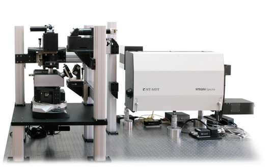
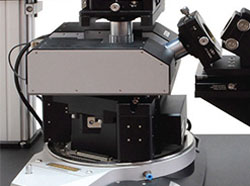
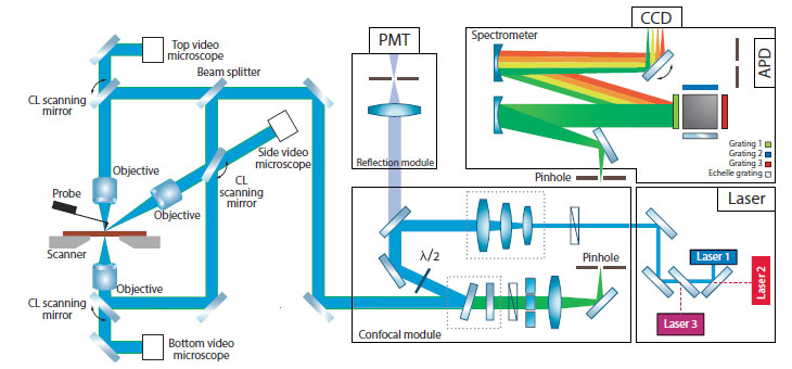
AFM-Raman, SNOM and TERS system
Versatile automated AFM-Raman, SNOM and TERS system


產品說明
Since 1998 NT-MDT has been successfully integrating AFM with optical microscopy and spectroscopy techniques. More than 30 basic and advanced AFM modes including HybriD ModeTM are supported providing extensive information about the sample surface physical properties. Integration of Simultaneously measured AFM and Raman maps of exactly the same sample area provide complementary information about sample physical properties (AFM) and chemical composition (Raman). |
NTEGRA Spectra II with the help of Tip Enhanced |
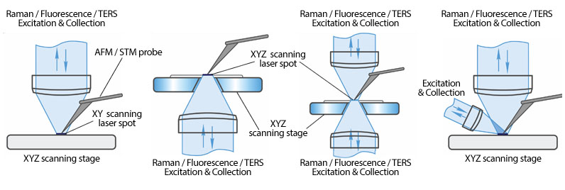
Solution for all possible excitation/detection and TERS geometries
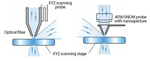
Aperture Scanning Near-Field Optical Microscopy
產品應用
|
|
|
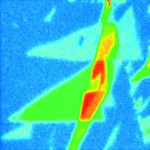
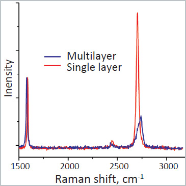
Graphene flakes
30x30 um |
Ni foil
20x20 um |
PC-PVAC film
30x30 um |
MoO3
30x30 um |
|
|||||||||
|
|
|
|
|
||||||
| Sample courtesy: prof. R. Carpick, Penn State University. Scan size 20x20 µm | |||||||||

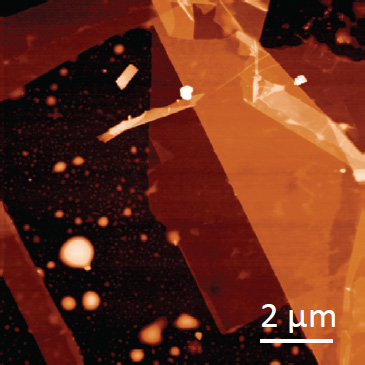
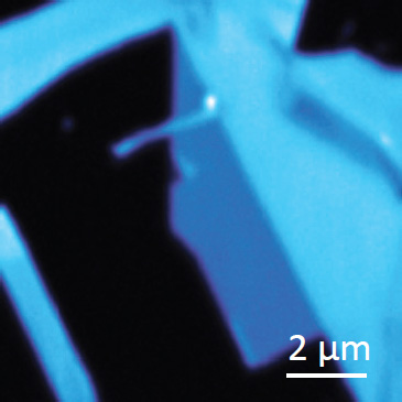
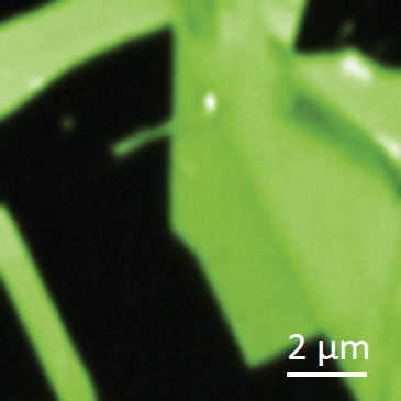
Graphene flake on Si/SiO2
|
|
|
|
|
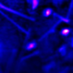
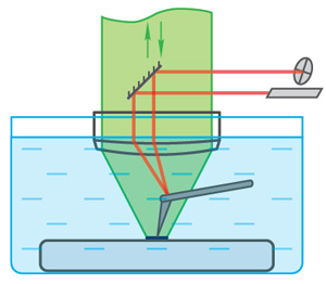
| TERS in liquid | ||
NT-MDT Spectrum Instruments has demonstrated enhancement of the Raman scattering (TERS) in application to an opaque sample - layer of organic dye deposed on a golden substrate - in liquid with the upright optical configuration NTEGRA Spectra II. Implementation of TERS in liquid brings out some difficulties. The main one is the delicate optical alignment to achieve accurate focusing of the laser beam on the tip apex and also to ensure an efficient collection of the scattered signal especially through a layer of liquid. In case of transparent samples set on an inverted optical microscope focusing of the laser beam on the TERS probe is therefore easily achieved directly through the sample. |
With opaque samples that require top or side illumination/collection, the optical signal is deviated and considerably attenuated by refraction at each interface. One of the possible ways to avoid refraction on air-liquid surface and to achieve stable light path is to use immersion objective. NTEGRA Spectra II is the only instrument which provides such possibility as AFM beam deflection system works through the same objective as Raman laser.
|
|
 |
 |
|
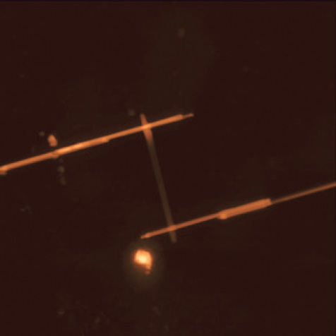
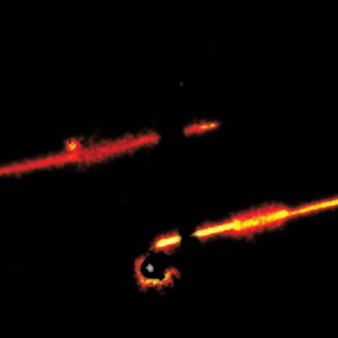
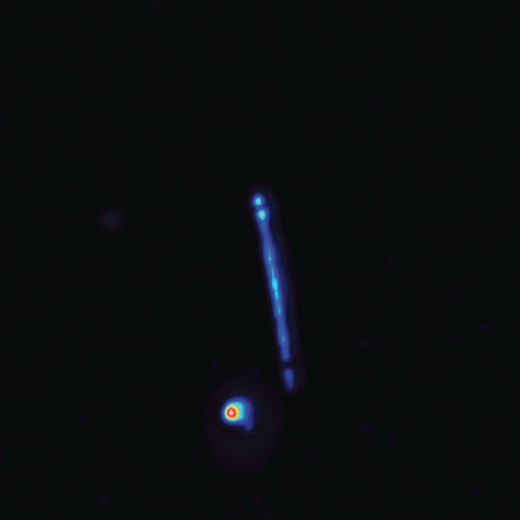
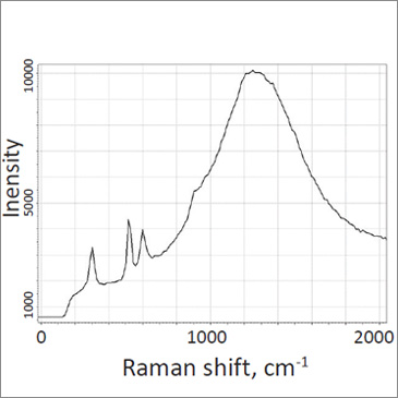
| During the experiment in AFM optical head a polarized excitation laser (λexc = 632.8 nm) was focused on the AFM TERS probe apex through a long distance 60× water immersion objective (working distance: 2 mm) with high numerical aperture (N.A. = 1). Therefore, the AFM tip holder can fit between the objective and the sample. Laser spot scanning was performed by scanning mirror. The enhanced spectrum and the one obtained from tip apex are presented in the figure and confirm the strong enhancement of the signal from around the “hot-spot” location. |

TERS (black) and microRaman (red) spectra
|
|
HybriD Mode™
Ntegra Spectra II equipped with new electronics and software allows to combine a recently developed innovative HybriD Mode™ (HD-AFM™ Mode) for nanomechanical proprieties and Raman for chemical imaging of exactly the same area within single measurement session.
 |
 |
 |
||
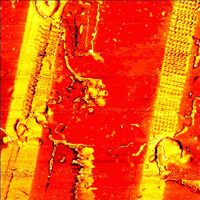
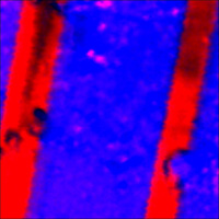
| Stiffness of HDPE/LDPE polymer sandwich cut by microtome | Overlap of Raman maps: HDPE (red), LDPE (blue) | AFM topography | ||
Image size: 34 × 34 μm Data from: M. Yanul, S. Magonov, P. Dorozhkin, NT-MDT. |
||||
Working principle
|
|
TERS Probes
- Cantilever-type, Excellent and Reliable
- Enhancement factors: 100x and more
- Lateral resolution in TERS: down to 10nm
- High speed TERS mapping
- Top-down illumination configuration (opaque samples)
- Based on commercial AFM cantilevers (contact, non-contact): multiple AFM modes, excellent imaging performance
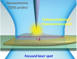
Introduction to TERS (nano-Raman)
Tip Enhanced Raman Scattering (TERS, nano-Raman) is the technique for enhancement of weak Raman signals and for super-resolution Raman imaging with spatial resolution ~10 nm. Nano-Raman imaging provides unique insights into sample structure and chemical composition on the nanometer scale.
In TERS, a sharp metal probe (nano-antenna) is used to localize and enhance optical field at the tip apex (fig. 1a). The light enhancement is typically reached when excitation laser light is in resonance with localized surface plasmon at the end of the TERS probe (fig. 1b). Enhancement of electromagnetic field (light) intensity on the TERS probe apex can reach many orders of magnitudes. In TERS mapping the sample is scanned with respect to the nano-antenna; the enhanced Raman signal localized near the probe apex is measured resulting in Raman maps of the sample surface with nanometer scale resolution.
 |
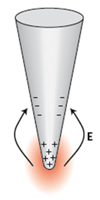 |
| Fig.1. Principle of Tip Enhanced Raman Scattering and other tip- assisted optical techniques (left). Localized surface plasmon (electron density oscillations) at the end of a metal TERS probe (nano-antenna), resulting in light localization and enhancement at the probe apex (right). | |
TERS (nano-Raman) imaging by NT-MDT AFM-Raman instrument
NT-MDT develops and supplies unique instrumentation for AFM integration with various optical microscopy and spectroscopy techniques. NT-MDT was the first to introduce integrated AFM-Raman instrument in 1998 and is now the leading developer and supplier of such instruments worldwide.
NT-MDT AFM-Raman instrument has been successfully used for TERS (nano-Raman) mapping of various objects with spatial resolution reaching 10 nm: graphene and other carbon nanomaterials, polymers, thin molecular layers (including monolayers), semiconductor nanostructures, lipid membranes, various protein structures, DNA molecules etc. References to corresponding publications can be found at download page.
TERS probe challenge
While the AFM-Raman instrumentation has been developing relatively fast, TERS probes have always remained main limiting factor for nano-Raman to become routine characterization technique. The main challenges are: (i) manufacturing reproducible probes with high enhancement factors and high resolution imaging capabilities; (ii) probe lifetime; (iii) probe ease of use; (iv) probe mass production not involving complicated and poorly reproducible manual procedures.
TERS probes originally used in scientific publications were usually etched metal wires - attached to tuning fork or working in STM (tunneling) regime. Preparation of such probes requires elaborated manual operations; probes are typically not very reproducible. Another approach to TERS probe preparation utilizes focused ion beam to manufacture special structure on the tip end. This approach is very resource consuming and also lacks reproducibility. Different metal coatings of AFM cantilevers have been reported recently – with different degrees of enhancements and reproducibility.
Reproducible TERS probes from NT-MDT
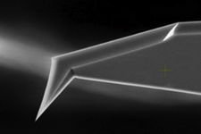
As a result of comprehensive research performed together with NT-MDT customers and partners, NT-MDT is now able to offer to its AFM-Raman customers mass produced reproducible cantilever-type TERS probes. The probes are prepared based on so-called “Top Visual” AFM Si cantilevers (Fig. 2). Special proprietary probe preparation and TERS metal coating are applied.
 |
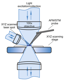 |
Fig. 2. SEM image of “Top Visual” AFM probe. Protruding probe geometry allows optical access to the apex from the top (left). Experimental TERS configuration (right). |
|
AFM probes can have different stiffness and can be optimized for contact and non-contact regimes.
Protruding “nose-type” shape of the probes allows Raman laser light to be focused on the probe apex from the top: for use with non-transparent samples.
The probes provide guarantied TERS performance on a test sample (organic molecules on Au substrate):
- Enhancement factor >50x (Tip IN vs. Tip. OUT) for ~70% of probes. Typical enhancement factor : > 100x. Some probes reach >500x enhancement.
- TERS (nano-Raman mapping). ~20-70 nm resolution. >50% of probes.
- Remarkable lifetime without considerable enhancement degradation
-
The AFM TERS probes also feature excellent AFM performance in contact and non-contact regimes since they are prepared based on standard Si AFM cantilevers produced by mass technology. All advanced AFM modes (electrical, magnetic, nanomechanical etc.) are available with NT-MDT TERS probes. High resonance quality factors (for non-contact probes) allow excellent force sensitivity and guarantee long tip lifetime during measurements.
STM TERS probes (electrochemically etched metal wires) and TERS probes attached to tuning fork are also available.
The NT-MDT TERS probes reach their highest characteristics with the unique AFM-Raman instrument from NT-MDT: specifically designed for TERS research.
Probes are only supplied to be used with NT-MDT instrumentation. Contact us for more information.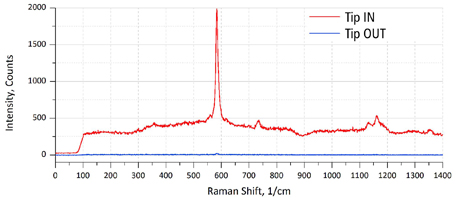

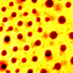
Fig. 3. Typical Raman signal enhancement (>100x) of NT-MDT TERS AFM probe (left). High resolution TERS map. Resolution: ~20 nm. Sample: BCB thin molecular layer on Au substrate (right). 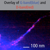
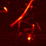
Fig. 4. High resolution TERS map of carbon nanotubes on Au substrate. Resolution: ~10 nm.
More technical information about TERS cantilevers: http://www.ntmdt-tips.com/products/group/ters-afm-probes-new
Downloads
- Characterization of Materials with a Combined AFM/Raman Microscope. Summary AN 089s
 (0,99 Mb)
 - Characterization of Materials with a Combined AFM/Raman Microscope AN 089 (1,18 Mb)
- Solar Cell Diagnostics by Combination of Kelvin Probe Force Microscopy with Local Photoexitation AN 091 (0,7 Mb)
- AFM-Raman Characterization of Pharmaaceutical Tablets AN 092 (0,7 Mb)
- AFM – Raman Characterization of Li-ion Batteries AN 093 (1,19 Mb)
- Interplay between Raman Scattering and Atomic Force Microscopy in Characterization of Polymer Blends AN 094 (0,9 Mb)
產品規格
| Confocal microscopy Confocal Raman/fluorescence/Rayleigh imaging runs simultaneously with AFM Diffraction limited spatial resolution: <200 nm in XY, <500 nm in Z (with immersion objective) True confocality; motorized confocal pinhole for optimal signal and confocality Continuously variable ND filter with the range 1-0.001 for precise change of laser power Motorized variable beam expander/collimator: adjusts diameter and collimation of the laser beam individually for each laser and each objective used Fully automated switching between different lasers - with a few mouse clicks Full 3D (XYZ) confocal imaging with powerful image analysis AFM/STM integration with spectroscopy High-performance low noise AFM: Z noise<0.1 nm (RMS in 10‑1000 Hz bandwidth) Easy-to-do exchange of registration system operational wavelength (670, 830, 1064 and 1300 nm). No interference between AFM laser and Raman spectroscopy Automated AFM laser, probe and photodiode positioning and alignment Objective-independent AFM registration system XYZ closed-loop sample scanner 100x100x10 μm Focus track feature: sample always stays in focus due to sample Z-feedback. High quality confocal images of very rough or inclined samples can be obtained Exchangeable probe holders (AFM, STM, Tuning fork). All standard SPM imaging modes are supported (including KPFM, SRI, PFM, SCM) and combined with confocal Raman microscopy A non-resonant oscillatory HybriD Mode™ allowing direct and fast force detection for quantitative and high-resolution mapping of local sample properties |
Spectroscopy Extremely high efficiency 520 mm length spectrometer with 4 motorized gratings Visible, UV and IR spectral ranges available Echelle grating with ultrahigh dispersion; spectral resolution: 0.007nm (< 0.1 cm-1) Up to 3 different detectors can be installed:
Flexible motorized polarization optics in excitation and detection channels, crosspolarized Raman measurements Low wavenumber/THz Raman spectroscopy: <10 cm-1 with Bragg volume filters Hyperspectral imaging (recording complete Raman spectrum in every point of 1D, 2D or 3D confocal scan) with further software analysis Light delivery system Optical access for top, bottom and side illumination at 30 degrees Highest possible resolution optics is used simultaneously with AFM: up to 1.45 NA for Inverted, up to 0.7 NA for Upright, up to 0.7 NA for Side configurations Exchangeable objectives with kinematic mounts: precision <2 µm Dual scan: scan by sample AND scan by laser spot (for Hot Spot mapping in TERS) Closed-loop scanning mirrors for precise laser spot positioning to the tip (important for SNOM, TERS): Upright, Inverted and Side configurations: 50×50 µm with 100× objective All SNOM signals are detected: laser intensity, fluorescence intensity, spectroscopy. All SNOM modes are supported: Transmission, Collection, Reflection, Scattering (s-SNOM) All existing TERS geometries are available: illumination/collection from bottom, from top or from side |